Quick answer
Field emission SEM, often called FESEM, is usually the better choice for advanced research imaging because it delivers a brighter electron beam, smaller probe size, and stronger low-voltage performance. Tungsten SEM is usually the better choice when the lab needs a lower-cost, robust, serviceable instrument for routine imaging, teaching, and general quality control.
The right choice depends on sample type, resolution requirement, analytical workflow, user skill level, and budget. A field emission source improves what the microscope can do, but it also raises expectations for vacuum quality, maintenance discipline, and operator training.
Key takeaways
- FESEM is preferred for nanoscale morphology, low-kV imaging, thin films, nanoparticles, semiconductors, polymers, and beam-sensitive specimens.
- Tungsten SEM is practical for fracture surfaces, particles, coatings, teaching, industrial inspection, and general materials work.
- The most important source-level difference is brightness, not just resolution.
- Tungsten SEM can perform useful EDX and routine analysis.
- FESEM often has higher purchase cost and more demanding service expectations.
- A lab should compare systems using its own samples, not only a vendor resolution standard.
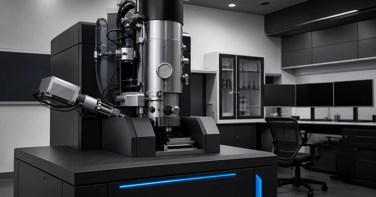
How tungsten SEM works
A tungsten SEM uses a thermionic electron source. A tungsten filament is heated until electrons are emitted. This is a proven and relatively simple source design. It is robust, familiar to many operators, and comparatively inexpensive to replace.
The tradeoff is that tungsten sources have lower brightness and a larger effective source size than field emission sources. The resulting probe is generally larger, especially at low accelerating voltage or low beam current. That limits ultimate resolution and can make fine surface imaging less crisp.
Tungsten SEM remains useful because many SEM tasks do not require the smallest possible probe. If the lab mostly images micron-scale features, coated biological samples, fracture surfaces, powders, fibers, corrosion layers, or production defects, tungsten SEM can provide excellent value.
How field emission SEM works
A field emission SEM extracts electrons from a very sharp tip under a strong electric field. In research instruments, the most common source is often Schottky field emission, which combines field-assisted emission with thermal stability. Cold field emission is another option and can provide very high brightness and narrow energy spread, although it may require more stringent vacuum and operational care.
The main benefits are:
- Higher brightness
- Smaller source size
- Better probe formation
- Improved low-voltage performance
- Better high-resolution imaging
- Higher useful probe current at small spot sizes
These advantages matter when the scientific question lives near the limit of surface detail, feature size, beam damage, or analytical spatial resolution.
Resolution and low-voltage imaging
Resolution is the most visible difference, but it should not be reduced to one number.
At higher accelerating voltages, both tungsten and field emission SEMs may produce useful images for many samples. The gap becomes more important at low accelerating voltage. Low-kV SEM is valuable because it reduces interaction volume and increases surface sensitivity. It can also reduce charging on some specimens.
Field emission sources generally maintain a smaller, brighter probe at low voltage. This makes FESEM more suitable for:
- Nanoparticles
- Thin films
- Semiconductor surfaces
- Polymer blends
- Battery materials
- Biological surface structures
- Fine coatings
- Beam-sensitive surfaces
For a researcher trying to image subtle surface morphology at 1 to 3 kV, FESEM is usually the stronger platform.
Probe current and analytical work
Analytical SEM is not only about imaging. EDX, EBSD, cathodoluminescence, and other techniques need enough signal to produce reliable data.
Tungsten SEM can be entirely adequate for EDX when the features are large enough and the required spatial resolution is moderate. Many routine industrial labs use tungsten SEM for elemental screening, contamination analysis, and failure analysis.
FESEM becomes more attractive when the lab needs a small probe with useful current. That combination is important for high-resolution EDX mapping, small particles, thin layers, or beam-sensitive samples where the operator wants to avoid simply increasing voltage or spot size.
For EBSD, the source choice is only one part of the system. Pattern quality also depends on sample preparation, stage geometry, detector position, beam current, and software. Still, field emission instruments are often preferred for demanding EBSD because they can provide stable current and a fine probe.
Stability and maintenance
Tungsten filaments are consumables. They are relatively inexpensive and familiar, but they burn out and require replacement. Brightness changes over filament life, and operators may need to realign the source after replacement.
Field emission sources last longer, but they are more expensive and tied more closely to vacuum health. A field emission SEM requires disciplined operation, clean samples, proper pumping, and service support. Source replacement or major service can be costly.
For a shared facility, this difference affects policy. A FESEM may need stricter user training and sample screening. A tungsten SEM may tolerate rougher routine use, although contamination and poor sample preparation still cause problems.
Cost and ownership model
Tungsten SEM usually has a lower purchase price and lower entry cost. It is often easier to justify for teaching labs, small industrial groups, and facilities that need general SEM access rather than frontier imaging.
FESEM costs more, but it can be the better investment when the lab needs:
- High publication-quality image resolution
- Low-kV surface imaging
- Nanomaterials characterization
- Semiconductor inspection
- Advanced analytical integration
- High-end detector configurations
- Shared core facility capability
The total cost should include service contracts, source lifetime, vacuum maintenance, detector service, software licenses, training time, and sample preparation tools.
Which source is better for which lab?
Choose field emission SEM when:
- The lab studies nanoscale or near-surface structures.
- Low-voltage performance is central.
- Users need high-quality images for publication.
- Small feature EDX or EBSD is important.
- The facility can support stronger training and maintenance practices.
Choose tungsten SEM when:
- Most features are larger than the nanoscale limit.
- The lab needs routine imaging and inspection.
- Cost control is a primary constraint.
- The instrument will be used heavily by students or occasional users.
- Maximum low-kV resolution is not essential.
Common search question: FESEM vs SEM
People often search for "FESEM vs SEM", but that wording is slightly imprecise. FESEM is a type of SEM. The real comparison is usually field emission SEM vs thermionic SEM, or field emission SEM vs tungsten SEM.
This distinction matters because an SEM can also differ by chamber size, detector package, vacuum mode, stage design, software, EDX integration, and service model. The source is important, but it is not the whole instrument.
Practical evaluation checklist
Before buying or booking time on either instrument, test:
- Your actual sample at your intended accelerating voltage
- Low-kV surface detail
- Image stability over a long acquisition
- Charging behavior without excessive coating
- EDX count rate and map quality
- Stage navigation and repeatability
- Ease of alignment and daily startup
- Software export and metadata quality
The best comparison is not theoretical. It is the image, spectrum, or map produced from the specimen that matters to your research.