Quick answer
SEM works by focusing a beam of electrons into a tiny probe, scanning that probe across a sample, and detecting signals created when the beam interacts with the sample. The instrument builds the image point by point, matching signal intensity to beam position.
The result is a detailed map of surface topography, composition, or both, depending on the detector and settings.
Key takeaways
- SEM images are scanned signal maps, not ordinary photographs.
- The electron gun produces the beam.
- Electromagnetic lenses focus and shape the beam.
- Scan coils move the beam across the sample surface.
- Detectors collect secondary electrons, backscattered electrons, X-rays, or other signals.
- Vacuum, sample preparation, and beam settings strongly affect image quality.
The SEM workflow in one pass
A typical SEM imaging sequence looks like this:
- The electron gun emits electrons.
- The instrument accelerates the electrons down the column.
- Condenser lenses and apertures shape the beam.
- Objective lenses focus the beam into a small probe.
- Scan coils sweep the probe across the sample.
- The beam interacts with atoms in the sample.
- Detectors collect emitted or scattered signals.
- Software converts signal intensity into an image.
Every pixel in an SEM image corresponds to a beam position and a detector response.
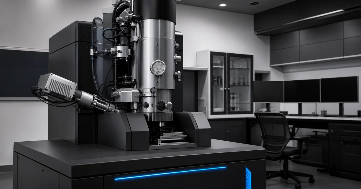
The electron source
The electron source is the starting point of SEM imaging. It produces the electrons that become the scanning beam.
Common SEM sources include:
- Tungsten filament sources
- Lanthanum hexaboride sources
- Schottky field emission sources
- Cold field emission sources
Field emission sources can produce a smaller, brighter, more stable beam than conventional tungsten sources. That often improves resolution, especially at low accelerating voltage or high magnification.
The electron column
The electron column controls the beam before it reaches the sample. It contains electromagnetic lenses, apertures, alignment controls, and scanning components.
The goal is simple in concept but demanding in practice: deliver a stable, focused probe to the sample.
Important column variables include:
- Probe size
- Beam current
- Aperture size
- Lens alignment
- Stigmation
- Working distance
- Accelerating voltage
Small changes in these settings can change image sharpness, signal strength, charging behavior, and analytical performance.
Beam scanning
SEM does not illuminate the whole sample at once. It scans a small beam across the surface in a raster pattern, similar in concept to how older displays scanned lines across a screen.
At each point, a detector measures signal intensity. The SEM assigns that intensity to the corresponding pixel. Higher signal often appears brighter. Lower signal appears darker.
Magnification in SEM is controlled by scan size. If the beam scans a smaller area of the sample while the image display remains the same size, the apparent magnification increases.
Beam sample interaction
When the electron beam enters the sample, it interacts with atoms in a small region called the interaction volume. The size and shape of that volume depend on accelerating voltage, atomic number, density, tilt, and sample composition.
The interaction produces several useful signals:
- Secondary electrons
- Backscattered electrons
- Characteristic X-rays
- Auger electrons
- Cathodoluminescence in some materials
Routine SEM imaging usually focuses on secondary and backscattered electrons. EDX analysis uses characteristic X-rays.
Secondary electron imaging
Secondary electrons are low energy electrons emitted from near the sample surface. Because they escape from a shallow depth, they are very sensitive to surface structure.
Secondary electron imaging is often chosen for:
- Surface roughness
- Fracture morphology
- Biological textures
- Insect features
- Fibers and powders
- Fine edges and pores
Edges and tilted surfaces often appear bright because they emit or release more detectable secondary electrons.
Backscattered electron imaging
Backscattered electrons are incident beam electrons that scatter back out of the sample. Heavier elements tend to produce stronger backscatter signals than lighter elements.
Backscattered electron imaging is often chosen for:
- Atomic number contrast
- Multiphase materials
- Polished sections
- Mineral grains
- Metal alloys
- Inclusion analysis
- Phase distribution
Backscattered images can look less surface dramatic than secondary electron images, but they often contain valuable compositional information.
X-ray analysis with EDX
The same beam interactions can produce characteristic X-rays. An EDX or EDS detector measures X-ray energies and uses them to estimate elemental composition.
EDX can answer questions such as:
- Is this particle rich in iron, silicon, calcium, or chlorine?
- Is a contaminant organic, mineral, or metallic?
- Do two phases have different elemental signatures?
- Does a coating contain the expected elements?
EDX has limits. It is affected by interaction volume, peak overlap, surface geometry, sample preparation, detector geometry, and standards. Still, it is one of the most useful analytical tools attached to SEM.
Why vacuum matters
Electrons scatter easily in air. A conventional SEM uses vacuum so the beam can travel from the electron gun to the sample with minimal interference.
Vacuum also helps stable operation of the electron source and detectors. However, vacuum can be difficult for wet, oily, porous, or biological samples. For those cases, some instruments offer low vacuum, variable pressure, or environmental SEM modes.
Sample preparation
The best SEM settings cannot fully rescue a poorly prepared sample.
Common preparation steps include:
- Mounting the sample securely
- Drying biological or wet samples
- Coating nonconductive samples with gold, platinum, carbon, or another conductive film
- Polishing cross sections
- Cleaning contamination
- Grounding the sample to the stub
- Choosing a suitable sample height
Preparation is not just a lab chore. It directly affects charging, resolution, contrast, contamination, and whether the image represents the real structure.
Important SEM settings
Accelerating voltage
Accelerating voltage controls electron energy. Higher voltage can increase penetration and X-ray generation. Lower voltage can improve surface sensitivity and reduce charging or beam damage for some samples.
Working distance
Working distance is the distance between the objective lens pole piece and the sample surface. Shorter working distance can improve resolution in many imaging modes, while longer working distance may be useful for EDX geometry or large samples.
Beam current
Beam current affects signal strength. Higher current can improve signal and EDX count rate, but it may reduce fine probe performance or damage sensitive samples.
Dwell time
Dwell time is how long the beam spends on each pixel. Longer dwell time can improve signal to noise, but it increases exposure and may worsen drift, charging, or contamination.
What can go wrong
Common SEM problems include:
- Charging on nonconductive samples
- Beam damage
- Hydrocarbon contamination
- Poor focus
- Astigmatism
- Vibration
- Drift
- Incorrect detector choice
- Overinterpretation of contrast
Good SEM practice is a mix of instrument skill and scientific caution. The sharpest image is not always the most accurate image.
How to read SEM method details
When a paper or lab report includes SEM images, useful method details include:
- Instrument model
- Electron source type
- Accelerating voltage
- Detector type
- Working distance
- Vacuum mode
- Sample coating
- Magnification and scale bar
- EDX conditions, if used
These details help readers judge image quality, compare results, and reproduce the work.