What magnification calibration actually verifies
The magnification displayed on an SEM screen (e.g., "10,000×") is a software-driven label. It corresponds to a specific scan-rate and field-of-view setting derived from the column's design parameters. But the actual imaging scale — the real distance on the sample corresponding to a given distance on the screen — depends on many parameters that drift over time, change with operating conditions, and aren't perfectly predictable from manufacturer specifications.
Calibration verifies the actual scale, with reference to known dimensions traceable to a national metrology institute (NIST in the US, PTB in Germany, NPL in the UK, NMIJ in Japan, etc.). The output is a calibration factor — how much the displayed magnification needs to be multiplied to match reality — and an uncertainty for that factor.
Without calibration, an SEM produces images at "approximately the indicated magnification, give or take a few percent." With calibration, the magnification is known with quantified uncertainty (typically 0.5-2% for well-calibrated instruments).
Why magnification drifts
Several mechanisms cause SEM magnification to deviate from nominal:
Working-distance dependence: changing the distance from final pole piece to sample alters the imaging geometry. Same magnification setting at different working distances = different actual scales.
Accelerating-voltage dependence: lens focal lengths depend on beam energy. The same lens current focused at 5 kV produces a slightly different magnification than at 30 kV.
Lens-current calibration drift: the current-to-focal-length relationship can drift due to lens-coil aging, temperature variations, magnetic hysteresis effects.
Scan-system calibration drift: the deflection coils that scan the beam over the sample area can have non-linearities and drifts.
Thermal effects: the column heats up during operation; thermal expansion can subtly affect geometry.
Software/firmware updates: occasionally bring magnification baseline changes that require re-calibration.
Maintenance / repair: replacement of any column component typically requires re-calibration.
Magnification errors of 1-5% are common in routine SEM operation; >5% typically signals a problem that needs investigation.
The reference standards
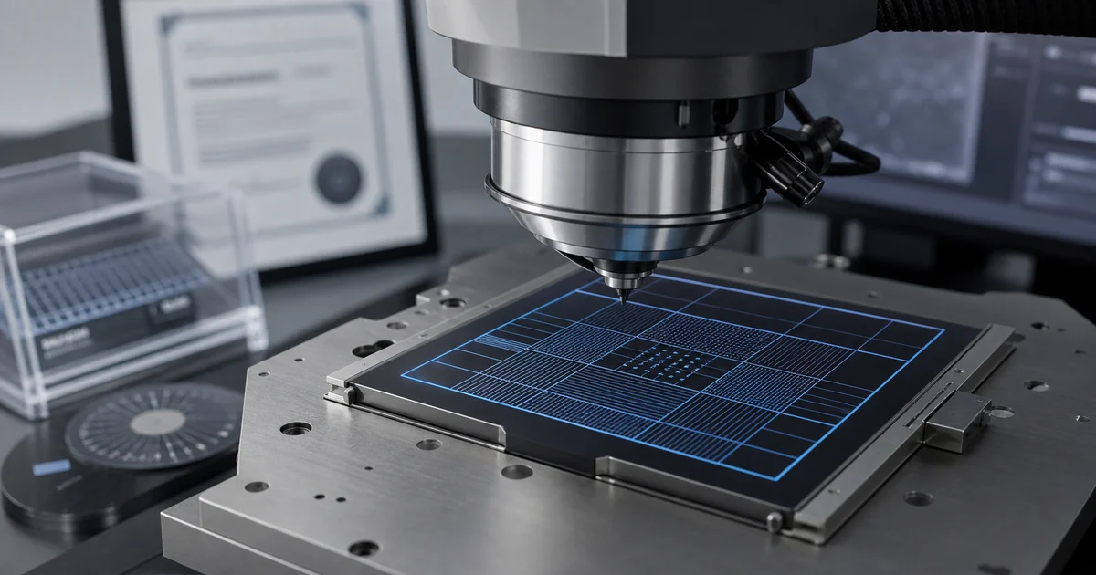
The certified reference standards used for SEM magnification calibration are precision-fabricated samples with known periodic structures (pitches) certified to traceable values:
NIST SRM 2090 and SRM 2091 (USA)
"Magnification Standard for Electron Microscopy" — silicon cross-grating reference materials issued by NIST specifically for SEM and similar electron-beam instruments. SRM 2090 covers larger pitches (mid-range SEM magnifications); SRM 2091 covers finer pitches (high magnifications). Each carries a NIST-issued certificate stating the pitch values with stated uncertainty, traceable to the SI meter.
NIST SRM 1963c
A silicon pitch standard with ~0.7 μm pitch features, commonly used for SEM and other length-metrology applications. Traceable to NIST.
NIST SRM 484 series
Glass line-spacing/line-width standards. Originally optical, but applicable across light and electron microscopy where appropriate scales fit.
BAM and PTB-traceable standards (Germany)
The Bundesanstalt für Materialforschung und -prüfung (BAM) and Physikalisch-Technische Bundesanstalt (PTB) issue traceable reference standards equivalent to the NIST options. Commonly used in European labs.
Commercial calibration grids
Several commercial suppliers (Geller MicroAnalytical, MicroToNano, Ted Pella, Aurion) provide pitch standards with NIST or PTB traceability:
- Geller MicroAnalytical X-1: silicon cross-grating, 1 μm and 0.2 μm pitches.
- MicroToNano: cross-grating samples at 0.2, 2.0, 5.0, 9.7 μm.
- Ted Pella: various calibration replica grids.
Each certificate identifies the chain of traceability (the metrology institute, calibration uncertainty, expiration if applicable).
Older but still relevant
Diatom samples: certain marine diatoms have nearly-perfect periodic structures and were used historically for magnification calibration. Largely superseded by manufactured standards but still occasionally referenced.
The calibration procedure (per ISO 16700:2016)
The international standard procedure:
Stable conditions: instrument warmed up, vacuum stable, sample chamber stabilized.
Mount reference: load the certified reference standard onto the stage.
Operating parameters: set the conditions you want to calibrate — accelerating voltage, working distance, aperture, magnification. Typical baseline: 10 or 20 kV, 10 mm working distance, mid-magnification (e.g., 1000× or 10,000×).
Focus and stigmate: bring the reference pattern into optimal sharpness. Astigmatism correction is essential — distorted images give wrong magnification.
Image acquisition: capture an image of the pattern at the operating magnification, avoiding drift. Fast scan rate or short integration recommended.
Measurement: using SEM software's measurement tool, measure pitch at multiple positions. ISO 16700 specifies at least 10 measurements per orientation (horizontal and vertical). Many labs measure 20-30.
Statistical analysis: compute mean apparent pitch (P_apparent) and standard deviation. The calibration factor is:
K = P_certified / P_apparent
Apply this factor to all subsequent measurements at the same conditions, or report it as the offset.
Repeat across operating conditions: do step 3-7 for each working distance, accelerating voltage, and magnification combination in your calibration table.
Documentation: record standard ID and certificate, operator, date, all operating conditions, measurement values, calibration factors, uncertainty.
Acceptance criteria: typically ±2-5% calibration tolerance per industry sector. Some semiconductor metrology requires <1%.
Working distance dependence
A common surprise: the same nominal magnification at 5 mm vs 15 mm working distance produces noticeably different actual scales. Magnitude varies by instrument (typically 2-10% over a 5-15 mm range).
For instruments that auto-correct for working distance, the correction is based on internal calibration tables that should themselves be calibrated and verified.
For instruments without auto-correction, the user needs to know which working distance the displayed magnification corresponds to (usually a specific "standard" WD) and apply correction factors at other distances.
Most modern SEMs report the calibration WD in their software documentation; if not, the manufacturer should be consulted.
Acceptance criteria
What counts as "acceptable" calibration?
Research-grade: ±5% is often fine. Many published images are uncalibrated to this level.
Semiconductor inspection / metrology: <1% is standard. Tight calibration is essential because dimensional measurements drive yield decisions.
Forensic / regulatory: <2-3% typical. Documentation and traceability are as important as the number.
ISO 17025 lab accreditation: institution-specific, but typically <1-3% with documented uncertainty budget.
Out-of-tolerance findings (calibration shifts beyond acceptance) trigger investigation:
- Re-measurement (was the procedure correct?).
- Mechanical inspection (aperture cleanliness, lens contamination, vacuum status).
- Service call if needed.
- All affected measurements since the previous good calibration are flagged for review.
Image rotation as part of magnification calibration
Beyond the scale factor, magnetic-lens imaging introduces an image rotation that depends on the lens current. Same magnification setting at different lens currents (different working distances) can produce images rotated by different angles relative to the stage.
For applications requiring orientation precision (anisotropic samples, crystal orientation analysis, defect orientation in semiconductor metrology), image rotation is calibrated alongside magnification — typically by imaging a reference sample with known orientation and recording the apparent angle.
A note on uncertainty
The calibration factor K has its own uncertainty:
u(K) = √[ (u(P_certified)/P_certified)² + (u(P_apparent)/P_apparent)² ]
where u(P_certified) is from the certificate (typically a fraction of a percent) and u(P_apparent) is from your measurement statistics.
The expanded uncertainty (typically reported at k=2, i.e., ~95% confidence) is 2 × u(K).
ISO 17025 calibration reports include this full uncertainty budget. Less formal use often quotes just the calibration factor without explicit uncertainty.
Automated calibration
Many modern SEMs have automated magnification calibration utilities:
- Operator loads a known reference standard.
- Instrument software automatically images, identifies the pattern, measures pitches, and updates the internal calibration table.
- Calibration history can be exported for QA records.
These work well for routine calibration but should be verified periodically against manual procedures and against new reference standards.
Optics physics in plain English
For readers wanting the foundational physics behind this:
The same principles of refraction-and-focus, aberration, and diffraction-limited resolution that govern optical microscopes apply to electron microscopes — just with electron beams instead of light. For an accessible introduction without metrology specifics, see Feynmanpedia's how lenses actually work and how microscopes work.
The takeaway
SEM magnification calibration uses certified reference standards (NIST SRM 2090/2091, SRM 1963c, or PTB-traceable equivalents) with traceable pitch values to verify and correct the instrument's actual imaging scale. ISO 16700:2016 specifies the canonical procedure: at least 10 measurements per orientation, statistical analysis, repeat at each operating condition (working distance, accelerating voltage, magnification). Working distance dependence makes multi-WD calibration essential for quantitative work. Acceptance criteria range from <1% (semiconductor metrology) to ~5% (research-grade). Image rotation is calibrated alongside magnification for orientation-critical applications. Full uncertainty budgets are part of ISO 17025 documentation. Modern instruments often automate the measurement; verification against manual procedures remains good practice.